A scanning electron microscope (SEM) is an electron microscope in which an electron beam is guided (rastered) in a certain pattern over the object to be enlarged and interactions between the electrons and the object are used to generate an image. The images generated with a scanning electron microscope are three-dimensional images of the object surface and have an extremely high depth of field.
We use the scanning electron microscope with EDX analysis / microanalysis for:
- Failure analysis, fracture analysis, wear analysis
- Damage by corrosion
- Damage caused by the effects of chemicals and other media on metals, plastics and elastomers
- Material determinations, analysis of surfaces
- Particle analysis
- Checking the manufacturing quality
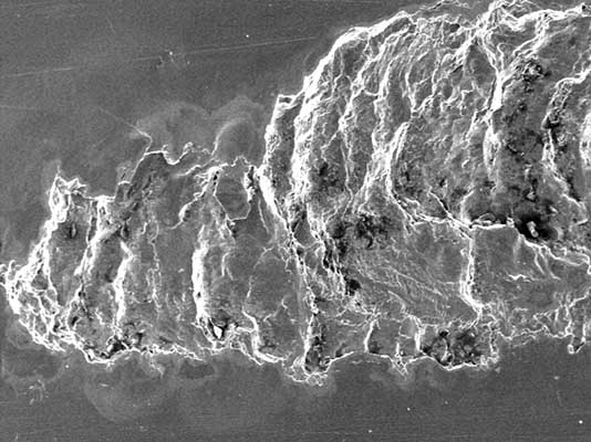
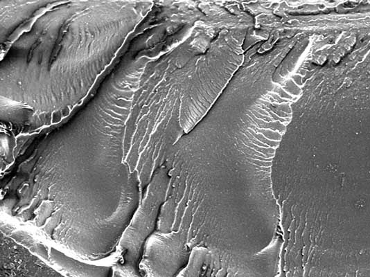
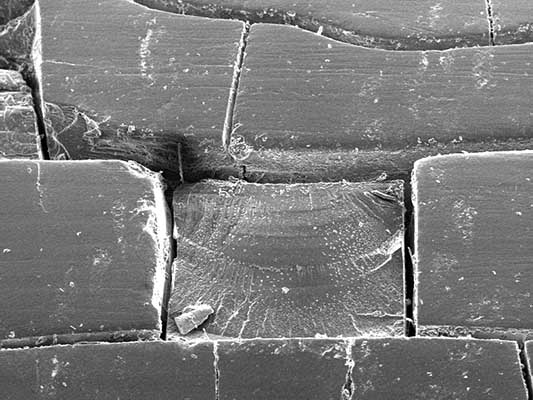
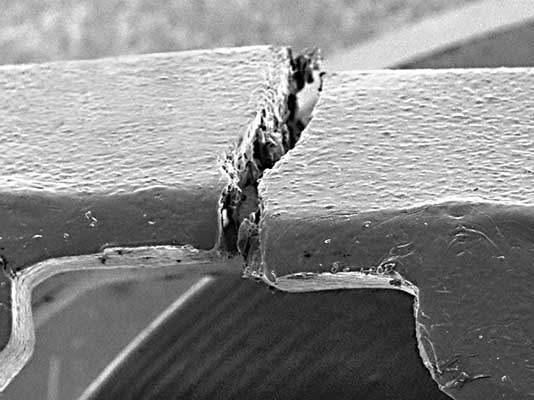
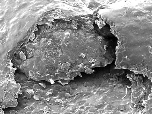
Damage analysis, breakage analysis, wear analysis
Using EDX analysis with SEM, traces of wear in a ball bearing can be shown vividly.
This is an important criterion for assessing damage.
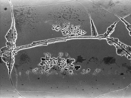
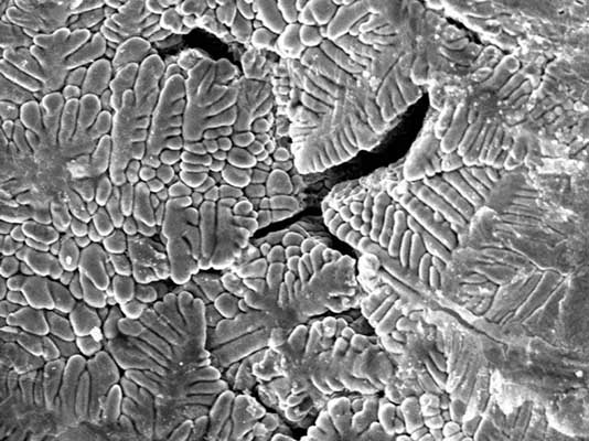
Corrosion damage
Corrosion occurs when a metallic material reacts with its environment and this reaction causes a measurable change in the material and can lead to an impairment of the function of a metallic component or an entire system.
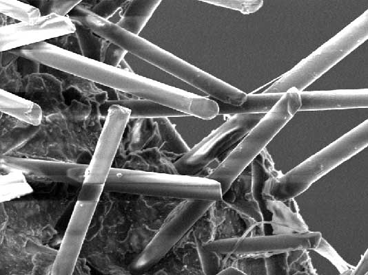
Damage caused by the effects of chemicals and other media on metals, plastics and elastomers
Components are exposed to various chemicals (grease, lubricants, coolants, solvents, cleaning agents) during their use.
These can trigger stress cracks in materials.
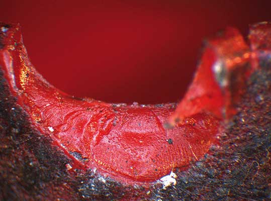
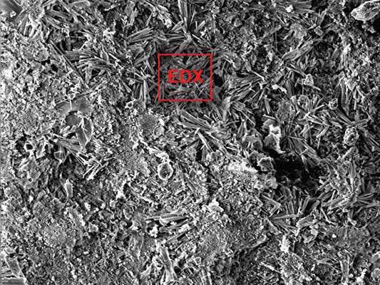
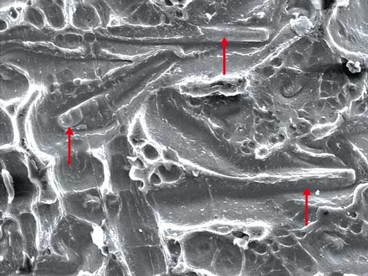
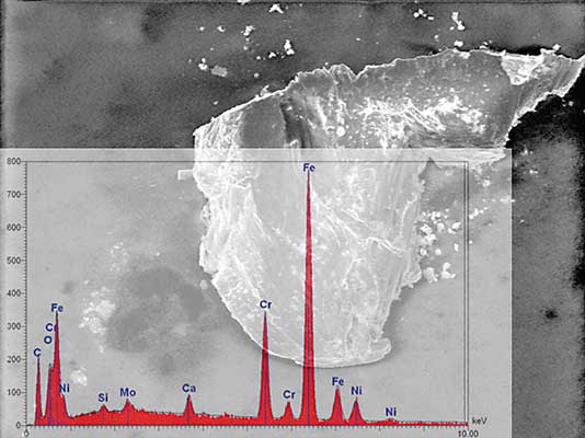
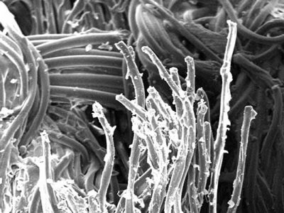
Material determinations, analysis of surfaces
Even tiny surface defects such as bubbles or craters can impair the visual impression when painting and coating components. While paint craters are caused, for example, by trace contamination with fats, oils or release agents, specks, pimples or other point elevations in the paint surface are often caused by the inclusion of foreign particles (dust particles, hair, fibers, metal abrasion).
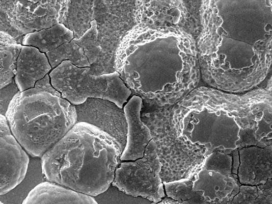
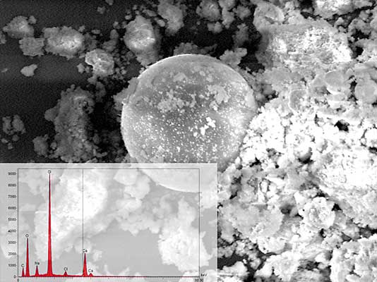
Particle analysis
The smallest particles can be to blame for the premature failure of a component. The IR microscope gives us useful results for particles up to 15 µm. Nevertheless, the use of a scanning electron microscope and EDX analysis is essential for inorganic substances.
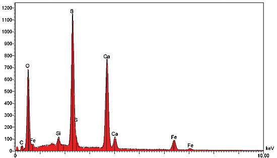
The EDX analysis detects the smallest elements that are contained in a sample. Electron microscopes are used for this, as they allow a significantly greater depth of field than light microscopes. For example, we can prove whether the particle is an impurity (foreign particle) or a filler particle that is too large.
Checking the manufacturing quality
The EDX analysis with SEM can also be used to check production quality, for example in the area of initial sample and series testing of components or assemblies.
FAQ
Small pieces up to approx. 50 × 50 × 20 mm, clean and dry. Non-conductive samples (plastic, ceramic) can be sputter-coated – please state whether the sample must be reusable afterwards. Do not clean fracture surfaces!
An individual EDX analysis with SEM images is often available in 3–5 working days. Extensive mappings / line scans 1–2 weeks.
Dekra Automobil GmbH, Unidekstraße 5, 75015 Bretten,
with the sample accompanying form (download area). Please state the suspected elements / question.
Typically 0.1–1 mass-% depending on the element and matrix; light elements (B, C, N, O) with higher uncertainty. For lower detection limits, we recommend ICP-OES or OES.
Yes, the combination of SEM image and EDX spectrum is an established means of evidence in complaint and court proceedings.